Hardware description
This page describes the hardware specifications and functionality of the expansion ports and how to use them.
Performance specification
| Component | Specification |
|---|---|
| CPU | NXP QorIQ LS1046A SoC: 4x Cortex-A72 @1.6 GHz |
| RAM | 8 GB ECC DDR4 @2100 MT/s |
| Networking | 2x SFP+ 10 Gbps (10GBASE-R) 3x RJ45 1 Gbps (1000BASE-T) |
| M.2 expansion* | 1x M.2_1 Key-E (Left) ‘Smart home’ – interfaces: SDIO, UART, SPI, I2C – Usage: low-bandwidth tri-radio cards (Wifi5, Bluetooth, Thread) 1x M.2_2 Key-E (Right) ‘Wireless’ – interfaces: UART, PCIe 3.0 x1 – Usage: Wifi6 2x2 MU-MIMO cards |
| Storage | User-selectable boot source via PCB dip-switch: 1x 64 MB NOR flash for Bootloader 1x 32 GB eMMC for Operating System |
| Firmware | NOR + eMMC (user-updatable) firmware targets are available — see Flashing firmware |
| Boot loader | U-Boot via booti |
| External I/O | 1x USB-C 3.1 5 Gbps port, max 5V 3A 1x USB-C UART (serial) console, 115200 baud ( ttyS0) |
| Internal I/O | 1x 4-pin 5V PWM CPU fan 1x 4-pin 5V header (unused) 1x programmable RGBW status LED 1x JTAG programmer connector 100+ PCB test points |
| Power supply (external) | 1x USB-C PD 3.0: 20V 2A (40W), or 15V 3A (45W) |
The Mono Gateway Development Kit is an extremely versatile device, and its design enables user recovery in an abnormally wide range of scenarios. Even if rendered ‘bricked’ and unbootable, the device can still be recovered via a separate JTAG hardware debugger probe (e.g. TC2050).
Port description
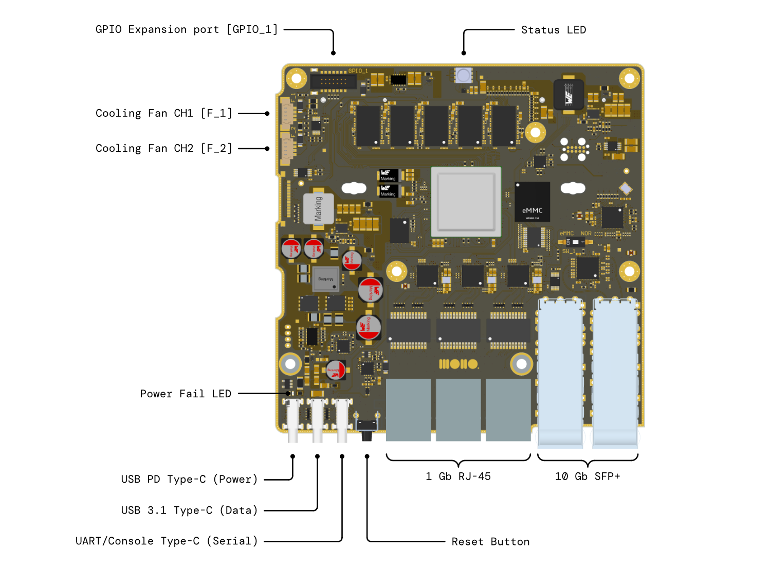
USB PD Type-C (Power)
Use the included 65W GaN power supply. Alternatively, any USB PD 3.0 compliant PSU rated for 15V 3A (45W) or 20V 2A (40W) or more will work. If the board doesn’t power up with a third-party adapter, it likely failed to negotiate sufficient power - this is indicated by the Power Fail LED diode.
Power Fail LED
Turned ON: Insufficient external USB power supply
Turned OFF: External power supply meets the required power needs. It is normal for the Power Fail LED to momentarily turn ON during the power up process.
USB 3.1 Type-C (Data)
A standard USB 3.1 host port. Use it to connect a thumb drive for backups, transfer files to/from the device, or attach external storage. Data speed 5Gbps. This port is designed to power an external device with 5V, up to 3A (15W).
UART/Console Type-C (Serial)
Your primary interface for communicating with the device, especially during initial setup. Connect this to your computer’s USB 2.0 port and use a serial terminal at 115200 baud. We recommend tio on macOS/Linux or PuTTY on Windows.
Reset Button
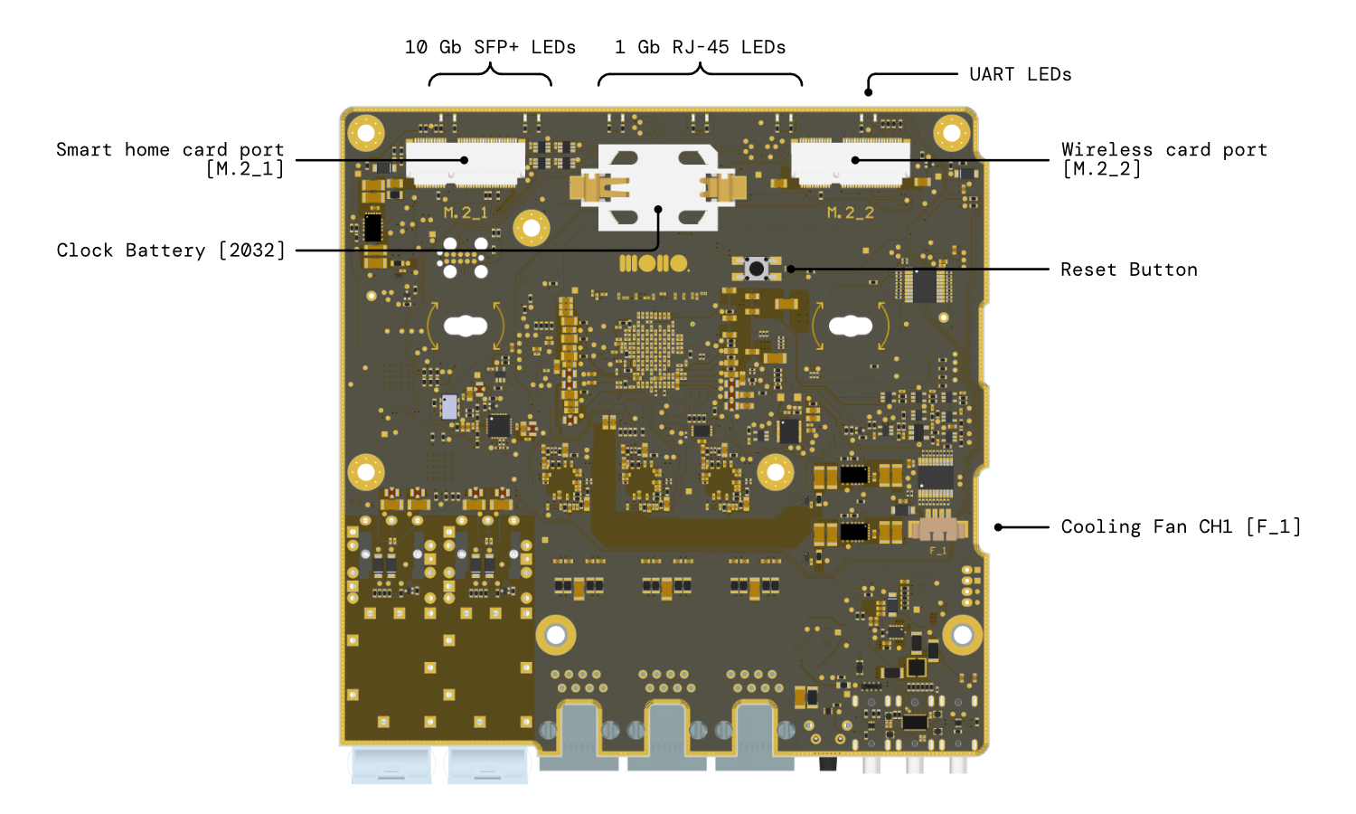
Resets the device by pulling the reset pin to ground on most chips. Note that this performs a reset, not a full power cycle. There are two reset buttons on the PCB, one located near the USB and network ports and the second one is located on the bottom side of the board near the RTC coin backup battery.
1 Gb RJ-45
Standard gigabit Ethernet ports, compatible with typical home networking equipment.
10 Gb SFP+
High-speed 10 gigabit ports for fiber or DAC connections. These should be compatible with a wide array of modules. If a particular module doesn’t work, it’s usually not a hardware limitation—the retimer chip is fully configurable via I2C, and our kernel configuration is open source.
Status LED
An onboard RGBW LED located on the top side of the board is directly controlled by the main processor. It is intended for system status indication and user defined signaling. More information about its behavior and control is provided in Getting started
Cooling Fan ports [F_1] & [F_2]
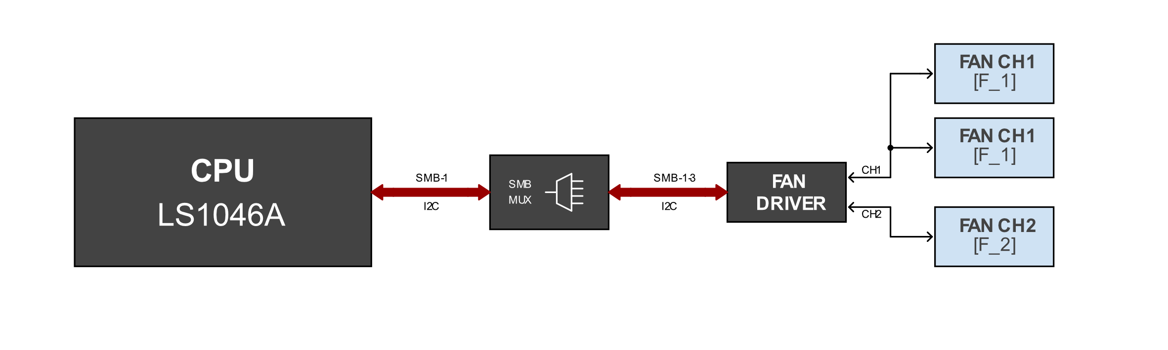
The cooling fan driver provides two fully independent channels designed to support 4-wire, 5 V cooling fans. These channels are labeled [F_1] and [F_2]. Channel 1 (CH1) has two physical connectors, one on the top side and one on the bottom side of the PCB, both labeled [F_1].
![Cooling Fan CH1 [F_1] & CH2 [F_2] pinout - PCB top side](/assets/development-kit-gpio-port-fan-4-wire-653104124022-pinout.png)
![Cooling Fan CH1 [F_1] pinout - PCB bottom side](/assets/development-kit-gpio-port-fan-4-wire-653104131822-pinout.png)

Connector type
| Connector type | Description | Link |
|---|---|---|
| PCB connector [F_1] | Wurth Elektronik 653104131822, 4-pin, 1.25mm | Datasheet |
| PCB connector [F_1] & [F_2] | Wurth Elektronik 653104124022, 4-pin, 1.25mm | Datasheet |
| Wire connector | Wurth Elektronik 620004113322, 4-pin, 1.25mm | Datasheet |
Pinout
From the Gateway port’s perspective
| Pin # | Name | Specification |
|---|---|---|
| 1 | GND | Power ground |
| 2 | +5V VCC | Power output, 5V, 250mA max per port. |
| 3 | TACH | RPM feedback input |
| 4 | PWM | PWM output signal |
GPIO Expansion port [GPIO_1]
The GPIO header can be found on the top side of the board and has 1.27mm pin pitch.

Connector type
| Connector type | Description | Link |
|---|---|---|
| PCB connector | Wurth Elektronik 62701420621, 14-pin, 1.27mm | Datasheet |
| Cable connector | Wurth Elektronik 62701423121, 14-pin, 1.27mm | Datasheet |
Pinout
A GPIO pin configured as an output pin can be set to high (1.8V) or low (0V).
A GPIO pin configured as an input pin can be read as high (1.8V) or low (0V). This is made easier with the use of internal pull-up or pull-down resistors. This can be configured in software.
From the Gateway port’s perspective
| Pin # | Name | Specification |
|---|---|---|
| 1 | PWR OUT 1.8V | Power output, 1.8V, 100mA max. Resettable fuse. |
| 2 | PWR OUT 3.3V | Power output, 3.3V, 100mA max. Resettable fuse. |
| 3 | I2C SDA | I2C BUS DATA. 1.8V logic level. |
| 5 | I2C SCL | I2C BUS CLOCK. 1.8V logic level. |
| 4 | GPIO_D1 | GPIO pin #1 |
| 6 | GPIO_D2 | GPIO pin #2 |
| 9 | GPIO_D3 | GPIO pin #3 |
| 10 | GPIO_D4 | GPIO pin #4 |
| 11 | GPIO_D5 | GPIO pin #5 |
| 12 | GPIO_D6 | GPIO pin #6 |
| 7-8, 13-14 | GND | Ground |
Voltage specifications
| INPUT | |
|---|---|
| Absolute maximum rating | 1.98 V |
| Input high voltage | >1.26 V |
| Input low voltage | <0.36 V |
| Input current | +-50 uA |
| OUTPUT | |
|---|---|
| Output high voltage | 1.35 V @ -0.5 mA |
| Output low voltage | 0.4 V @ 0.5 mA |
| Maximum current | +-0.5 mA |
M2 wireless card ports [M2_1] & [M2_2]
The Gateway includes two M.2 Key-E expansion ports that support two different categories of wireless cards:
| Card type | Features | Key type | Purpose | Port designation |
|---|---|---|---|---|
| Tri-radio | Wireless | Key-E | Home automation & smarthome | [M2_1] |
| Dual-radio | Wireless | Key-E | Main radio card for wireless | [M2_2] |
Supported cards
| Card name | Type | PCB port | Test status | Recommended to use |
|---|---|---|---|---|
| uBlox M2-MAYA-W271-00B | Tri-radio | [M2_1] | Basic HW & Firmware tests done. | YES |
| H&D Wireless SPB438-NTD | Tri-radio | [M2_1] | No tests performed yet | ON YOUR OWN RISK |
| uBlox M2-JODY-W377-00B | Dual-radio | [M2_2] | Basic HW & Firmware tests done. | YES |
| AzureWave AW-XM458MA-PUR | Dual-radio | [M2_2] | No tests performed yet | ON YOUR OWN RISK |
Pinout Tri-radio card [M2_1]
From the Gateway port’s perspective
| Pin # | Signal name | Description |
|---|---|---|
| 1, 7, 33, 39, 45, 51, 57, 63, 69, 75 | GND | Ground |
| 2, 4, 72, 74 | +3V3 VCC | Power output, 3.3V |
| 18 | VIO_CFG | Pulled to ground via 0R resistor |
| 9 | SDIO_CLK O (1V8L) | SDIO bus used for Wifi. Wifi card CLK input signal |
| 11 | SDIO_CMD I/O (1V8L) | SDIO bus used for Wifi. Wifi card CMD input/output signal |
| 13 | SDIO_D0 I/O (1V8L) | SDIO bus used for Wifi. Wifi card D0 input/output signal |
| 15 | SDIO_D1 I/O (1V8L) | SDIO bus used for Wifi. Wifi card D1 input/output signal |
| 17 | SDIO_D2 I/O (1V8L) | SDIO bus used for Wifi. Wifi card D2 input/output signal |
| 19 | SDIO_D3 I/O (1V8L) | SDIO bus used for Wifi. Wifi card D3 input/output signal |
| 22 | UART_RXD I (1V8L) | UART bus used for BT. Wifi card TXD output signal |
| 32 | UART_TXD O (1V8L) | UART bus used for BT. Wifi card RXD output signal |
| 38 | SPI MOSI O (1V8L) | SPI bus used for 802.15.4. Wifi card MOSI input signal |
| 40 | SPI MISO I (1V8L) | SPI bus used for 802.15.4. Wifi card MISO output signal |
| 42 | SPI CLK O (1V8L) | SPI bus used for 802.15.4. Wifi card CLK input signal |
| 62 | SPI_INT I (1V8L) | SPI bus used for 802.15.4. Wifi card INT output signal |
| 64 | SPI_FRM O (1V8L) | SPI bus used for 802.15.4. Wifi card FMR input signal |
| 58 | I2C_DATA I/O (1V8L) | I2C bus. Wifi card DATA input/output signal |
| 60 | I2C_CLK O (1V8L) | I2C bus. Wifi card CLK input signal |
| 23 | M2_3R_RESET O (1V8L) | Wifi card reset signal |
| 54 | M2_3R_RESET O (Open Drain) | Wifi card reset signal |
| 56 | M2_3R_nENABLE O (3V3L) | Wifi card power-down signal |
| 24-31 | M.2 Key E connector notch | Mechanical cutout in the M.2 card |
| Other pins | N.C. | Not connected |
Pinout Dual-radio card [M2_2]
From the Gateway port’s perspective
| Pin # | Signal name | Description |
|---|---|---|
| 1, 7, 33, 39, 45, 51, 57, 63, 69, 75 | GND | Ground |
| 2, 4, 72, 74 | +3V3 VCC | Power output, 3.3V |
| 18 | VIO_CFG | Pulled to ground via 0R resistor |
| 22 | UART_RXD I (1V8L) | UART bus used for BT. Wifi card TXD output signal |
| 32 | UART_TXD O (1V8L) | UART bus used for BT. Wifi card RXD input signal |
| 34 | UART_CTS I (1V8L) | UART bus used for BT. Wifi card RTS output signal |
| 36 | UART_RTS O (1V8L) | UART bus used for BT. Wifi card CTS input signal |
| 35 | PCIe TX0+ O (1V8L) | PCIe bus usef for Wifi. Wifi card RX0+ input signal |
| 37 | PCIe TX0- O (1V8L) | PCIe bus usef for Wifi. Wifi card RX0- input signal |
| 41 | PCIe RX0+ I (1V8L) | PCIe bus usef for Wifi. Wifi card TX0+ output signal |
| 43 | PCIe RX0- I (1V8L) | PCIe bus usef for Wifi. Wifi card TX0- output signal |
| 47 | PCIe REFCLK+ O (1V8L) | PCIe bus usef for Wifi. Wifi card REFCLK+ input signal |
| 49 | PCIe REFCLK- O (1V8L) | PCIe bus usef for Wifi. Wifi card REFCLK- input signal |
| 52 | M2_2R_RESET O (3V3L) | Wifi card reset signal |
| 54 | M2_2R_RESET O (3V3L) | Wifi card reset signal |
| 56 | M2_2R_ENABLE O (3V3L) | Wifi card power-down signal |
| 24-31 | M.2 Key E connector notch | Mechanical cutout in the M.2 card |
| Other pins | N.C. | Not connected |
Wireless card installation
TBD
RTC backup battery
The Real-Time Clock (RTC) circuit uses a coin cell battery to maintain time and date information when the device is powered off or disconnected from the main power source.
If the battery is removed or fully discharged, the RTC will lose its stored time and date, and the clock will need to be reset after the next power-up.
| Battery spec | |
|---|---|
| Model | CR2032 |
| Size | 20mm diameter |
| Nominal voltage / capacity | 3V / >150mAh |
| Rechargable | No |
Replacing the battery

To replace the battery, the PCB must first be removed from the enclosure. Follow the disassembly instructions provided below.
Once the PCB is accessible, use a flathead screwdriver to carefully lever the battery out of the holder, as shown in the image.
I2C / SMBUS Device tree
The board carries 22 I2C/SMBus devices, reached through four CPU built-in controllers and three bus multiplexers. The table below describes the device tree of the I2C system.
The CPU LS1046A provides four I2C controllers. IIC1, IIC2 and IIC3 each drive one TCA9545A 4-channel multiplexer, so every device on those buses sits behind one mux channel. The IIC4 is a single-device bus wired directly to the board EEPROM. All three multiplexers are strapped to the same address, 0x70.
| Bus / CPU channel | MUX (addr) | Device | Channel (reg) | Part number | Addr 7-bit | Addr 8-bit W/R |
|---|---|---|---|---|---|---|
| Bus 1 - SMBus (CPU IIC1) | ||||||
| 0x70 | mux itself | Texas Instruments TCA9545APWR | 0x70 | 0xE0 / 0xE1 | ||
| └─ 10GbE XFI-SFI retimer | CH0 (reg 0x01) | Texas Instruments DS100DF410SQ | 0x30 | 0x60 / 0x61 | ||
| └─ System clock generator | CH0 (reg 0x01) | Renesas 6V49205BNLGI | 0x69 | 0xD2 / 0xD3 | ||
| └─ Temperature sensor 1 - CPU diode | CH1 (reg 0x02) | Texas Instruments TMP431ADGKR | 0x4C | 0x98 / 0x99 | ||
| └─ Temperature sensor 2 | CH2 (reg 0x04) | Texas Instruments TMP431ADGKR | 0x4C | 0x98 / 0x99 | ||
| └─ Fan controller | CH3 (reg 0x08) | Microchip EMC2302-1-AIZL-TR | 0x2E | 0x5C / 0x5D | ||
| Bus 2 - I2C (CPU IIC2) | ||||||
| 0x70 | mux itself | Texas Instruments TCA9545APWR | 0x70 | 0xE0 / 0xE1 | ||
| └─ SFP+ port 1 module - pluggable | CH0 (reg 0x01) | - | 0x50 / 0x51 | 0xA0 / 0xA1 | 0xA2 / 0xA3 | ||
| └─ SFP+ port 2 module - pluggable | CH1 (reg 0x02) | - | 0x50 / 0x51 | 0xA0 / 0xA1 | 0xA2 / 0xA3 | ||
| └─ M.2 Key-E tri-radio card | CH2 (reg 0x04) | - | card dependent | |||
| └─ GPIO & PWR expansion header | CH3 (reg 0x08) | - | external | |||
| Bus 3 - I2C (CPU IIC3) | ||||||
| 0x70 | mux itself | Texas Instruments TCA9545APWR | 0x70 | 0xE0 / 0xE1 | ||
| └─ Power monitor - USB-PD input | CH0 (reg 0x01) | Texas Instruments INA234AIYBJR | 0x40 | 0x80 / 0x81 | ||
| └─ Power monitor - 5V0_SYS | CH0 (reg 0x01) | Texas Instruments INA234AIYBJR | 0x41 | 0x82 / 0x83 | ||
| └─ Power monitor - 1V_CPU_CORE | CH0 (reg 0x01) | Texas Instruments INA234AIYBJR | 0x42 | 0x84 / 0x85 | ||
| └─ Power monitor - 1V2_MEM | CH0 (reg 0x01) | Texas Instruments INA234AIYBJR | 0x43 | 0x86 / 0x87 | ||
| └─ Power monitor - 1V35_SERDES | CH1 (reg 0x02) | Texas Instruments INA234AIYBJR | 0x40 | 0x80 / 0x81 | ||
| └─ Power monitor - 1V8_SYS | CH1 (reg 0x02) | Texas Instruments INA234AIYBJR | 0x41 | 0x82 / 0x83 | ||
| └─ Power monitor - 2V5_SYS | CH1 (reg 0x02) | Texas Instruments INA234AIYBJR | 0x42 | 0x84 / 0x85 | ||
| └─ Power monitor - 3V3_SYS | CH1 (reg 0x02) | Texas Instruments INA234AIYBJR | 0x43 | 0x86 / 0x87 | ||
| └─ USB-C PD sink controller | CH2 (reg 0x04) | STMicroelectronics STUSB4500QTR | 0x28 | 0x50 / 0x51 | ||
| └─ Real-time clock | CH2 (reg 0x04) | NXP PCF2131TFY | 0x53 | 0xA6 / 0xA7 | ||
| └─ USB Type-C port controller | CH2 (reg 0x04) | Texas Instruments HD3SS3220IRNHR | 0x47 | 0x8E / 0x8F | ||
| └─ RGBW LED driver | CH3 (reg 0x08) | Texas Instruments LP5810AYBHR | 0x50-0x53 / 0x6C-0x6F | 0xA0 / 0xA1 | ||
| Bus 4 - direct (no mux) (CPU IIC4) | ||||||
| └─ Board EEPROM | no mux | Microchip AT24CS32-MAHM-E | 0x50 & 0x58 | 0xA0 / 0xA1 | 0xB0 / 0xB1 |
Disassembly instructions
Since the expansion features are not accessible with the enclosure installed, it is mandatory to remove the printed circuit board (PCB) from the enclosure.
Before disassembling the device, ensure that proper ESD safety precautions are followed to prevent damage to the electronics.
PCB removal guide
Required tools
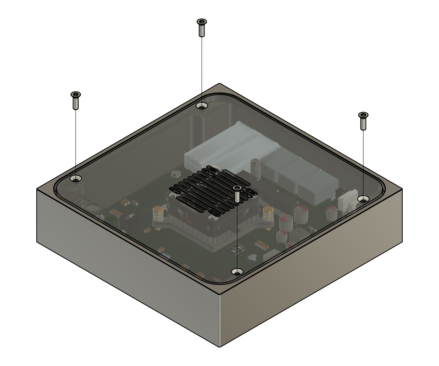
Torx T10 screwdriver
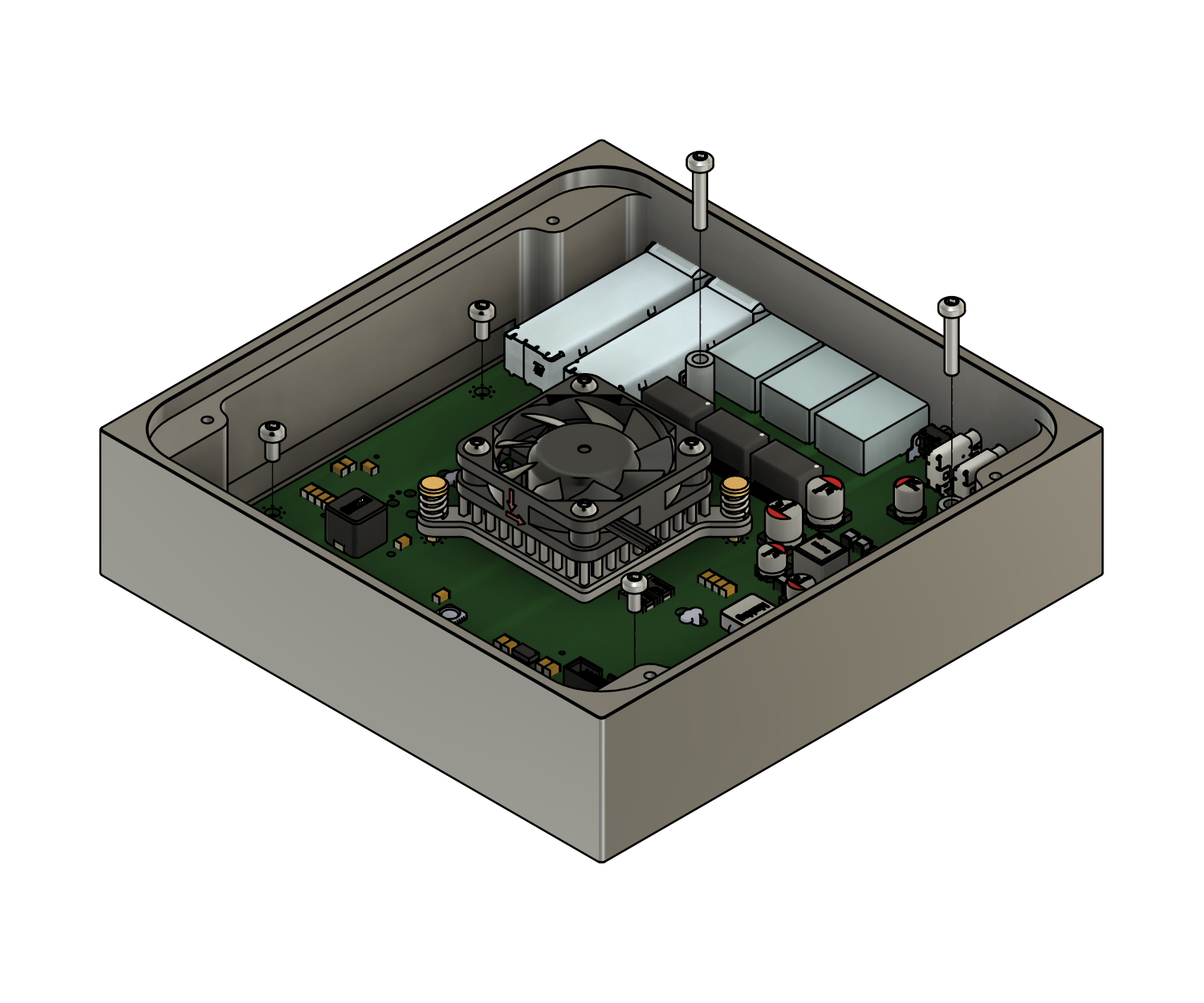
Steps
- Power off the device and disconnect all cables.
- Place the device on a clean, flat, and ESD-safe surface.
- Using a Torx T10 screwdriver, remove the four screws securing the top cover of the enclosure.
- Carefully lift and remove the top cover.
- Using the same Torx T10 screwdriver, remove the five screws that secure the PCB to the enclosure.
- Gently lift the PCB out of the enclosure, holding it by the edges only.
ESD safety notes
- Work on an ESD-safe surface whenever possible.
- Wear a grounded ESD wrist strap, or regularly touch a grounded metal object to discharge static electricity.
- Avoid touching components, connectors, or exposed contacts on the PCB.
- Store the PCB in an ESD-safe bag when it is not installed in the enclosure.
PCB mechanical properties
![Development Kit PCB dimensions - mm [in]](/assets/development-kit-pcb-dimensions.png)
PCB thickness is 1.6mm [63 mil]
Download 10G_GW_DK_PCB_3D-STEP.zip
Power Supplies Test Points
The Gateway development kit supports basic hardware diagnostics through direct measurement of its onboard power supply outputs. The accompanying PDF and Excel files identify the measurement test points and specify the acceptable voltage range for each supply rail.
How to measure
- Use a digital multimeter configured for DC voltage measurement, with a measurement range above the expected rail voltage.
- For easier measuring, remove the PCB from its enclosure first.
- Power up the Gateway Router.
- Connect the negative probe to a board ground (GND) reference and place the positive probe on the corresponding voltage test point
- Compare each measured voltage against the specified minimum and maximum limits. A reading outside these limits may indicate a power supply fault, excessive loading, or an issue with the input power source and warrants further investigation. Measurements within the specified limits confirm the DC voltage levels at the tested points.
Download Test Points Positions
Download Test Points Voltage Ranges
Development Kit enclosure
Here you can download the 3D step models of the Development Kit enclosure (top and bottom part).